4 Physical Design Cycle The input of the physical design cycle is a circuit diagram and the output is the layout of the circuit. The tool calculates max.

Mantra Vlsi Crosstalk Questions
Certainly one of the most well-liked nail art enhancements unfortunately 3D nail art will also be one of the most time consuming to perform.

. Up to 10 cash back Performance Power and Area are the three main pillars of the Chip Design Crosstalk can hamper all three. Presented at the 1999 International Conference on VLSI Design. Crosstalk is a phenomenon by which a logic transmitted in vlsi circuit or a netwire creates undesired effect on the neighbouring circuit or netswires due to capacitive coupling.
To achieve a efficient Chip design which give the best performance uses optimal power and in minimal Chip. 12 DECEMBER 1999 1817 Short Papers Crosstalk in VLSI Interconnections Ashok Vittal Lauren Hui Chen Malgorzata Marek-Sadowska Kai-Ping Wang and Sherry Yang Abstract We address the problem of crosstalk computation and. If the value of IR drop is more than the acceptable value it calls.
From the below picture we can see that. Crosstalk minimisation using vlsi. What are VIAs in VLSI.
VLSI physical design interview questions and answers. This noise is called as crosstalk noise. These values are defined so that optimization and analysis can ensure that the spurious signals.
This video covers the basics that you need to start with analysing crosstalk noise crosstalk delay reports in VLSI Digital IC Designs. VIAs in VLSI. These are basically called as VIAs.
Noise margin is the amount of noise a circuit can withstand without compromising its operation. Crosstalk delay depends on the switching direction of aggressor and victim net because of this either transition is slower or. It implies the delay happening in the output transition of victim due to transition of aggressor.
This unwanted element is called Signal Integrity. IR drop determines the level of voltage at the pins of standard cells. To connect between different metal layers we need poly layer along with the metal layers that we are going to connect.
The crosstalk analysis and the routing tool described in this paper were used in three generations of VLSI processor chip designs for IBMs S390 computers always. Crosstalk is a phenomenon by which a logic transmitted in vlsi circuit or a netwire creates undesired effect on the neighboring circuit or netswires due to capacitive coupling. Lets consider a buffer that is placed in a common path both data path and clock path for buf2 and buf3 buffer.
The aggressor net has a rising transition at the same time when the victim net has a falling transitionThe aggressor net switching in the opposite direction increases the delay for the victim. Crosstalk Noise Model for Shielded Interconnects in VLSI-basedCircuits Junmou Zhang and Eby G. Koehl Analysis reduction and avoidance of crosstalk on VLSI chips in Proceedings of the International Symposium on Physical Design 1998 doi.
When you perform crosstalk analysis using PrimeTime SI a change in delay due to crosstalk along the common segment of a clock path can be pessimistic but only for a zero-cycle check. Crosstalk in vlsi physical design Create captivating 3D nail art designs with 3D Nail Art Jewelry from The Nail Superstore. CRPR and Crosstalk Analysis.
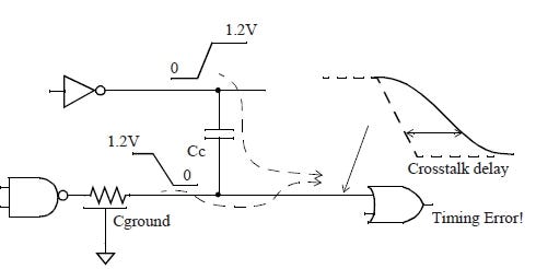
Refer to the digram below to get a clear picture on the effect of coupling capacitance on functionality and timing of VLSI circuits. What Is the Importance of IR Drop Analysis. Due to the influence of cross coupling capacitance switching of the signal from one net aggressor to the neighboring net victim.
He is a Physical Design Engineer in eInfochips working in the backend design domain. Not obscure the physical. If we have crosstalk then we might lose data or gain some extra datalogic which was not required.
Delays for setup calculation and min. In VLSI we have same situation with the nets routed that even nets are at their track but impacted by the noise from other nets. Minimisation of crosstalk in VLSI 1 Presented By.
And it also explains. IEEE TRANSACTIONS ON COMPUTER-AIDED DESIGN OF INTEGRATED CIRCUITS AND SYSTEMS VOL. This video will give you a quick overview of various fixing methods that can be applied during eco implementation phase in ASIC physical design in VLSIFollo.
Subhradeep Mitra Ankita Dutta Paramita Sau Debanjana Biswas Mca Students of Rajabazar sc. During the transition on adjacent signal aggressor net causes a noise bumpglitch on constant signal victim net. This is known as crosstalk.
Value of acceptable IR drop will be decided at the start of the project and it is one of the factors used to determine the derate value. Erich Klink of the VLSI Packaging and Physical Design depart- ment layed the basics to initially consider crosstalk an important as- pect of advanced chip physical design. Delays for hold worst- and best-case analysis.
The positive crosstalk impacts the driving cell as well as the net interconnect - the delay for both gets increased because the charge required for the coupling capacitance Cc is. Signal integrity and crosstalk are quality checks of the clock routes. Friedman Department of Electrical and Computer Engineering University of Rochester Rochester New York 146270231 Abstract Placing shields around a victim signal line is a common way to enhance signal integrity while minimizing delay uncertainty.
Crosstalk occurs via two mechanisms. Crosstalk in VLSI interconnections. In the next section we would discuss the crosstalk mechanism in VLSI Design.
Crosstalk is the interference caused due to communication between the circuits Lets learn to HOW TO REDUCE CROSSTALK. Refer to the diagram below to get a clear picture on the effect of coupling capacitance on functionality and timing of VLSI circuits. Sini Mukundan January 25 2017.

Team Vlsi Crosstalk Noise And Crosstalk Delay Effects Of Crosstalk
Crosstalk Analysis And Its Impact On Timing In 7nm Technology By Einfochips An Arrow Company Medium

Crosstalk Analysis And Its Impact On Timing In 7nm Technology By Einfochips An Arrow Company Medium

Optimization Of Crosstalk Delta Delay On Clock Nets
Cts Part Ii Crosstalk And Useful Skew Vlsi Physical Design For Freshers

Vlsi Crosstalk Analysis In Physical Design Crosstalk Noise Crosstalk Delay Fixing Crosstalk Youtube

Team Vlsi Crosstalk Noise And Crosstalk Delay Effects Of Crosstalk

Cts Part Ii Crosstalk And Useful Skew Vlsi Physical Design For Freshers
0 comments
Post a Comment